Case Study: High-Speed Camera Helps Push Limits on Semiconductor Metrology
New experiments from a Netherlands-based research institute depend on Emergent’s high-speed image capture to mitigate vibration challenges in a novel overlay metrology concept.
To keep up with Moore’s Law — a cornerstone of innovation that predicts that the number of transistors on a microchip will double approximately every two years — the semiconductor industry continues to push up against fundamental limits. This is the wheelhouse in which the Advanced Research Center for Nanolithography (ARCNL) in Amsterdam lives — among the extreme scientific challenges that make this industry tick.
In this world of semiconductor fabrication, the smallest of vibrations can cause the largest of problems — namely, having to scrap a processed wafer that could be worth thousands of dollars. Working to solve future technical challenges in the area of semiconductor chip manufacturing, ARCNL has developed a method to overcome the inherent sensitivities in the kinds of interferometric techniques the equipment maker will need to ensure accuracy in chip manufacturing.
Fulfilling the Promise of Digital Holographic Microscopy
As circuit sizes continue to shrink, digital holographic microscopy (DHM) has been shown to be a promising interferometric measurement technique for future overlay metrology. DHM would be used to measure the accuracy of the alignment of chip layers on semiconductor wafers. However, the technique is inherently sensitive to undesired phase variations, leading to image quality distortion caused by mechanical vibrations and air turbulence.
DHM works nicely in a lab environment, but implementing it in the real world is where it gets tricky, notes Tamar Cromwijk, a researcher at ARCNL and PhD student at the Vrije Universiteit in Amsterdam, and lead author on a research article published in the Oct. 7 issue of Optics Express. “In the real world, the precision of interferometric methods like DHM is impacted by vibrations,” she says.
In a high-throughput production environment, a semiconductor wafer moves at rapidly varying velocities in a metrology tool, resulting in large accelerations, and that causes the biggest concerns for vibration, Cromwijk explains.
“It is a huge technical challenge that we need to solve. You want to be as quick as possible with your metrology, so you have to start measuring while mechanical vibrations are present. So that’s cause number one,” she says. Other vibrations, such as temperature fluctuations and the movement of fans, also contribute to the problem. “It all contributes to a total phase fluctuation that degrades the measurement quality, and that’s what we are trying to mitigate.”
Along with the Dutch Research Council, the University of Amsterdam, Vrije Universiteit, and the University of Groningen, ARCNL operates in direct partnership with an equipment manufacturer, which sees potential in DHM if its limitations can be overcome.
High-Speed Camera Enables Correction
To correct the contrast loss created by vibrations, ARCNL researchers have come up with a method based on high-speed computational correction of the impact of vibrations. A high-speed camera is used to capture a sequence of digital holograms to track vibration as a function of time. By tracking and interpolating the phase changes between exposures, the system can compensate for the loss of image contrast in the holograms. Ultimately, this leads to improved imaging for more precise overlay measurements.
“If we track that phase over time, then we can correct for it afterwards. But we can only track what the vibrations were doing if we are faster than the vibration itself,” Cromwijk says. “So that’s what we need the high-speed camera for — to isolate and follow the behavior of the phase of the vibrations.”
In both its experimental interferometric setup and its vibration mitigation setup in DHM, the research team is using an HZ-2000-G-M 100GigE camera from Emergent Vision Technologies, which has a Gpixel GSPRINT4502 CMOS image sensor. At full resolution (2048 x 1216 pixels), the camera achieves 3462fps in 8-bit mode and 1782fps in 10-bit mode. For this work, the researchers are running the camera at 1000fps in 10-bit mode.
The high speed and high resolution of the camera are both critical for this experimentation, Cromwijk says. “We have a 2.5 megapixel sensor, and the ability to read all that information at such a high speed, that is not something every camera can do,” she says. “It’s the speed, resolution from the small pixels, and then the ability to read out 250 frames in one buffer, so we can measure over quite a long time.”
The compact size of Emergent’s camera is important as well. The ARCNL team looked into other high-speed cameras, but not only were they very expensive, Cromwijk says, they were huge. “We cannot put it in a breadboard, and we like to demonstrate that our solution is cost-effective without sacrificing performance.”

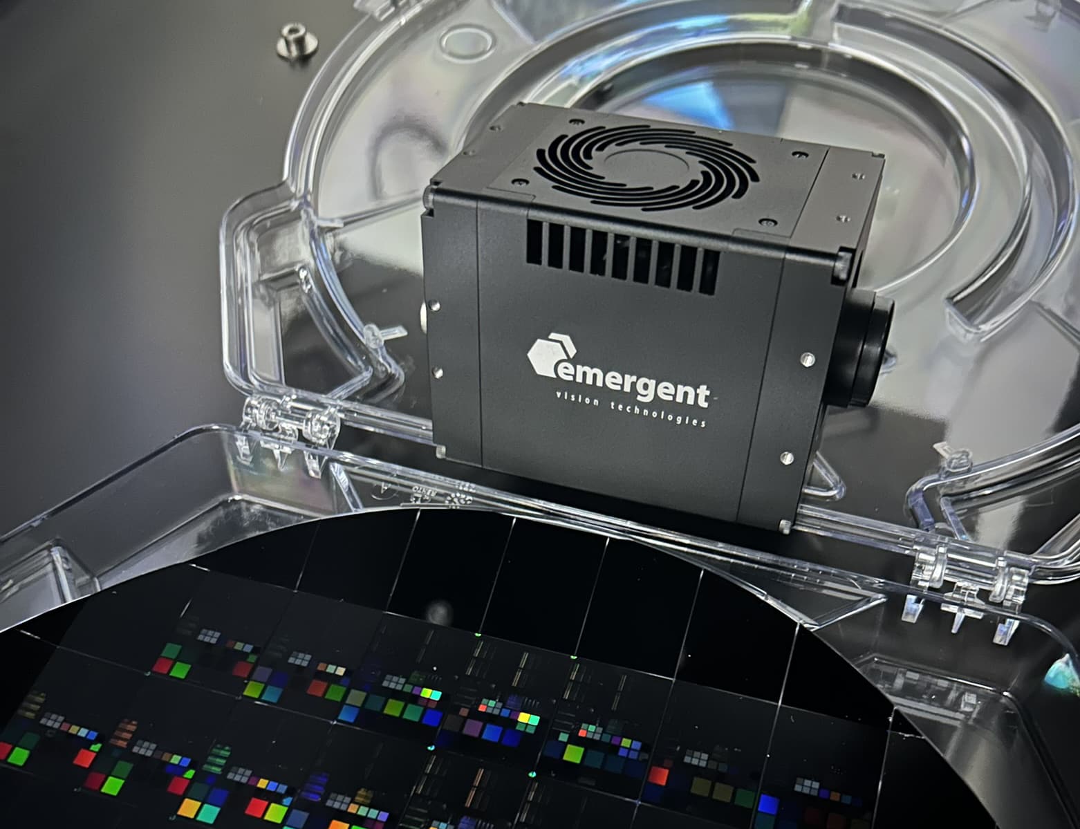
Figure 1: In the lab at the Advanced Research Center for Nanolithography (ARCNL), researchers use a high-speed camera to track and correct phase variations caused by mechanical vibrations during digital holographic microscopy (DHM).
The DHM Setup
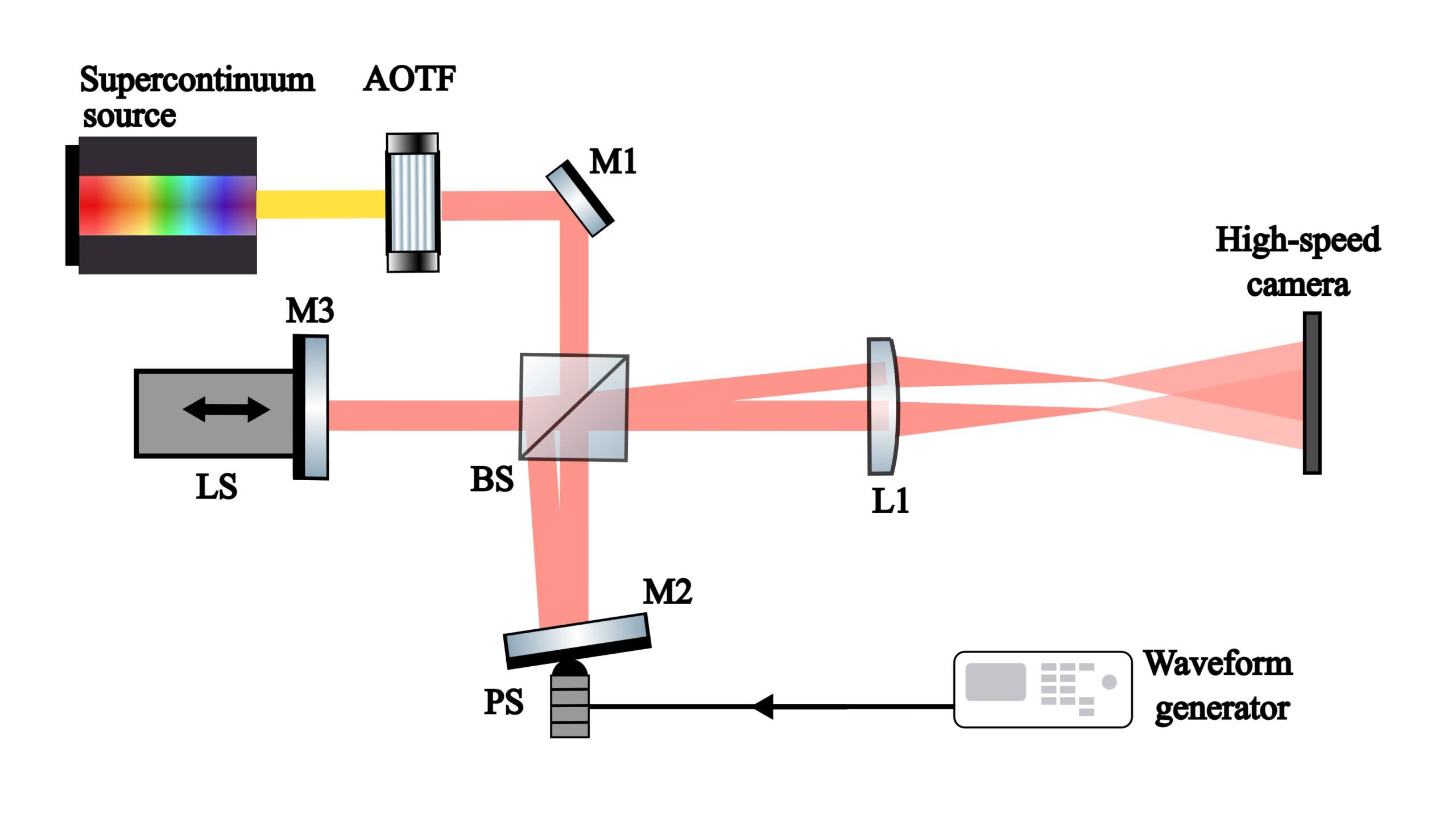
ARCNL researchers first verified the concept of their vibration mitigation technique on a simple Michelson interferometer setup. In this process, light from a supercontinuum white light source is filtered by an acoustic optical tunable filter (AOTF) to get the desired wavelength. With a 50:50 beamsplitter, the 632 nm beam is divided into an illumination beam toward one mirror and a reference beam toward another mirror. Placing the first mirror at a small angle creates a dense fringe pattern, similar to a fringe pattern in off-axis holography. Beyond the beamsplitter, a lens images the mirror surfaces on the high-speed camera. The team controls optical path lengths by moving the first mirror, where they also add a piezoelectric stack to create vibration.
After that initial verification, ARCNL performed an overlay measurement using a dark-field off-axis DHM on dedicated test targets. In a similar setup, the DHM uses a fiber-coupled supercontinuum white light source that’s spectrally filtered by an AOTF to a 632 nm wavelength with a bandwidth of 3 nm. In this case, the beam intensity is split using a 90:10 beamsplitter to create an illumination and reference beam, respectively. A nonpolarizing 50:50 beamsplitter is used in both paths for parallel acquisition of the +1st and −1st diffraction orders.
Ultimately, a sequence of holograms is captured with the Emergent high-speed camera. Each hologram yields a retrieved phase, which is then interpolated to retrieve the continuous phase variation, which is then used to calculate contrast loss.
In addition to its speed and compact size, the HZ-2000-G-M integrates GPUDirect technology, allowing the captured data to be transferred directly to the GPU for real-time processing. This capability significantly reduces latency and maximizes the efficiency of data handling, which is critical for the large amounts of data generated by the camera.

Figure 2: The setup includes a supercontinuum white light source, an Acousto-Optic Tunable Filter (AOTF) for wavelength selection, a 50:50 beamsplitter to split the beam, and a waveform generator to control vibrations via a piezoelectric stack for interferometric measurements.
Moving Forward With Advanced Imaging Capabilities
Such an experiment could not have been achieved without the progress of camera technology over the past several years. “This is something which was not possible 10 years ago, and that’s because of the amount of data which we can read out from the camera,” Cromwijk says. “For example, 10 years ago, we might have been able to do the same with one line, but now we can have the full field of images.”
The experimental concept is designed for not only the resolution needed for the ever-smaller circuits of future semiconductors but also a broader wavelength range to look at multiple colors at the same time. The third goal is weak targets, Cromwijk explains. “If you have, for example, an opaque layer in between, where the scattering from your grating below is very weak, with this holographic technique, you can put more light in your reference beam, and then you basically amplify your whole signal,” she says.
Noting the success of initial experiments in achieving more precise overlay metrology, the researchers also note further improvements that could be made to the technology. As Emergent continues to make improvements to its capabilities, Cromwijk is keeping in touch with the camera supplier to stay on top of developments in frame rates, pixel sizes, bit depth, and more. While 100GigE is the focus now, Emergent is far from done. Stay tuned for even more groundbreaking developments in 2025.
For full details of the experiments and results, read the research article from ARCNL.
FOR FURTHER INFORMATION:
Emergent Vision Technologies’ High-Speed Cameras:
https://emergentvisiontec.com/area-scan-cameras/


